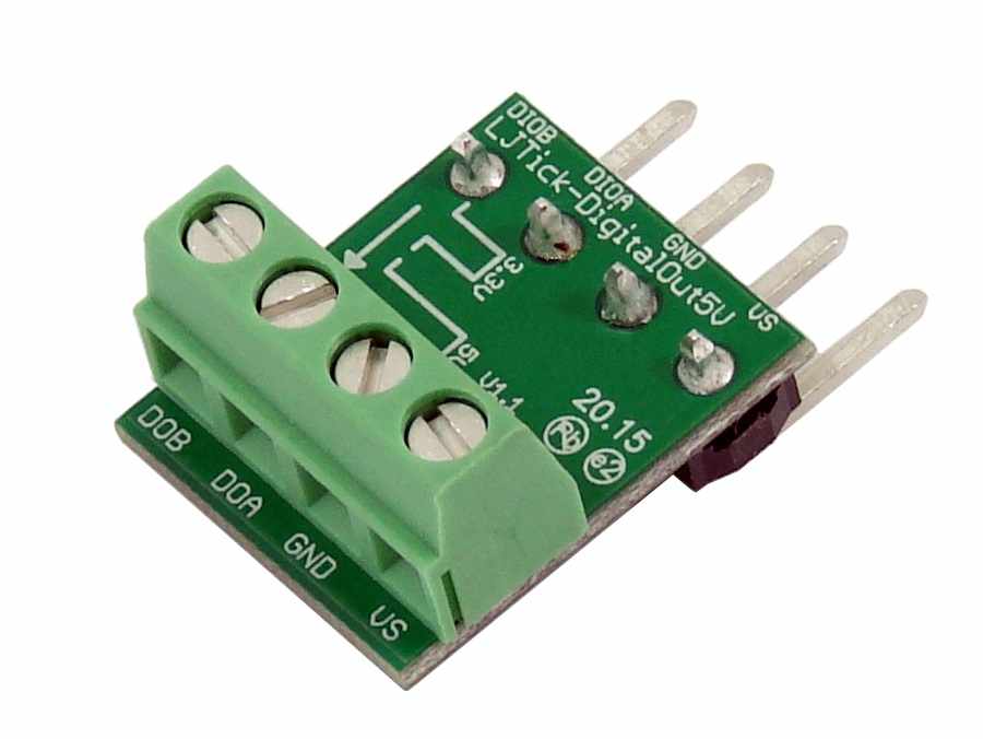
The LJTick-DigitalOut5V (LJT-DO5V) converts a LabJack's 3.3V digital outputs to 5V digital outputs. This allows a LabJack device to control 5V relays or interface with 5V logic devices/sensors. Read more about controlling relays and connecting 5V signals in this app-note.
-
Output only
-
Source or sink 50mA or more
-
Up to 800kHz
-
Interfacing with 5V logic circuitry
Note: When the LabJack digital I/O is configured as an input, the DigitalOut5V accessory will output logic low.
Common Applications
-
Controlling relays that require 5V logic signals.
Screw Terminal Descriptions
VS: This is the same 5 volt output as the VS terminals on the LabJack itself. This is an output terminal, not an input. It can be used to provide 5 volt (nominal) power as needed.
GND: Same as LabJack ground (GND).
DOA/DOB: These lines are the converted 5V logic lines.
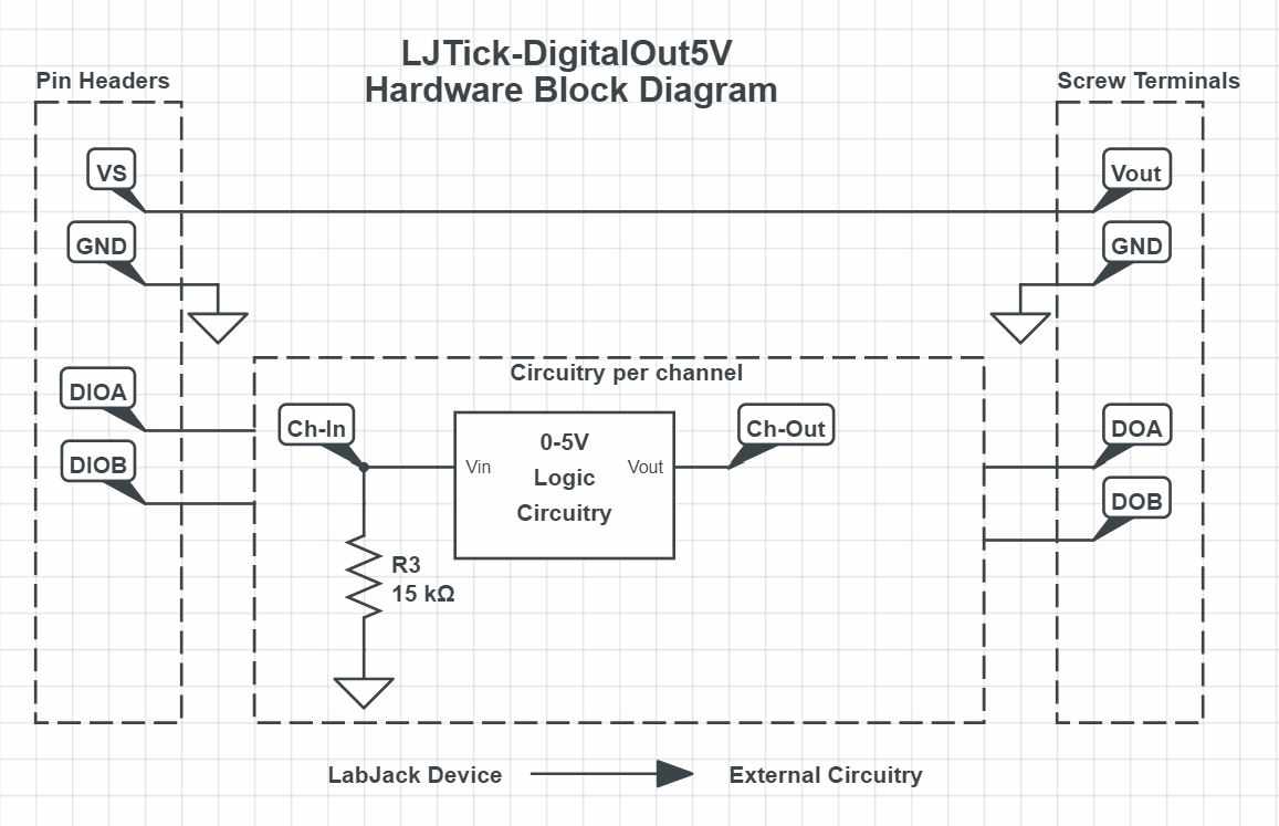
LJTick-DigitalOut5V Hardware Block Diagram

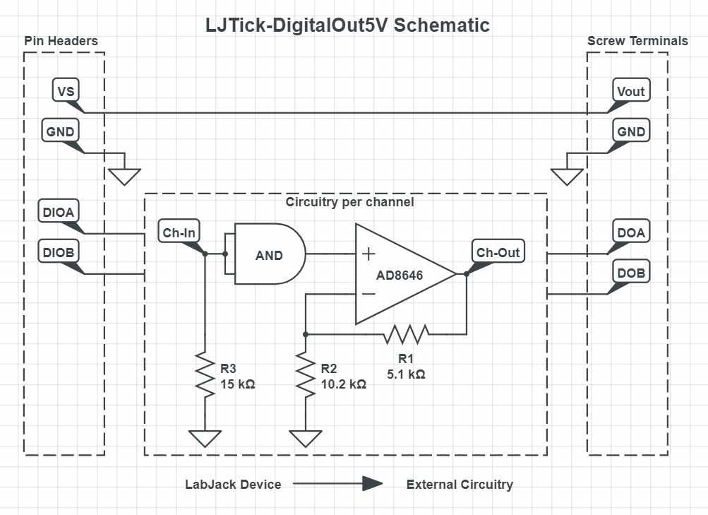
LJTick-DigitalOut5V Schematic

The AND gate has Schmitt trigger inputs (i.e. hysteresis), which help avoid rapid toggling if a noisy signal slowly changes state.
The AND gate is powered by 3.3 volts from a regulator. An input of 0 to 1.0 volts will cause the output of the AND gate to be 0 volts. An input of 2.3 to VS (nominally 5.0) volts will cause the output of the AND gate to be 3.3 volts.
The output amp is powered by VS & GND, and is set up with a gain of x1.5. Thus the 3.3 volt high output of the AND gate will result in a 5.0 volt output from the amp, assuming a light load and assuming that VS is at least 5.0 volts.
If the DIO connected to the tick's input is set to output-high, the tick's output will be high. It the DIO is set to output-low, the tick's output will be low. If the DIO is set to input, the tick's output will be low (due to the pull-down resistors on the inputs). This last fact can be useful when the DIO is configured to go to output-low at power up, as there is usually a brief time where the line will be input before the configuration takes effect.
Specifications
|
Parameter |
Conditions |
Min |
Typical |
Max |
Units |
|
|
|
|
|
|
|
|
Supply Voltage |
|
3.5 |
|
5.25 |
Volts |
|
Supply Current |
No loads |
|
1.5 |
|
mA |
|
Operating Temperature |
|
-40 |
|
80 |
°C |
|
|
|
|
|
|
|
|
Input Range |
Normal |
0 |
|
VS |
Volts |
|
|
Max |
-0.5 |
|
VS+0.5 |
Volts |
|
Input to cause Logic high |
|
2.3 |
|
|
Volts |
|
Input to cause Logic Low |
|
|
|
1.0 |
Volts |
|
|
|
|
|
|
|
|
Logic High Output |
VS = 5.0V |
|
5.0 |
|
Volts |
|
Logic Low Output |
|
|
0 |
|
Volts |
|
Logic High with Load |
VS = 5.0, 50 mA load |
|
4.6 |
|
Volts |
|
Output Drive Current (1) |
Sink or Source |
|
50 |
|
mA |
|
Rise Time Delay |
|
|
70 |
|
ns |
|
Fall Time Delay |
|
|
90 |
|
ns |
|
Rise Time |
|
|
380 |
|
ns |
|
Fall Time |
|
|
460 |
|
ns |
|
Max Frequency (2) (3) |
|
|
760 |
|
kHz |
(1) Short circuit current is 120 mA, but useable current varies with how close to rail you need to drive per Figure 13 of the AD8646 datasheet. Figure 13 applies to both rails and applies to sinking or sourcing. For example, if driving high and sourcing 50 mA there will be a saturation voltage of about 400 mV so the output will be about 4.6V rather than 5.0V.
(2) This is the recommended maximum frequency of a square wave of 50% duty cycle if the required output signal needs to get to both 0V and 5V. Faster frequencies will result in the signal not reaching 0V.
(3) An output frequency of 1MHz with both voltage rails being met can be achieved by using a duty cycle of 45%. The output waveform will look like a triangle wave at this point with the specified rise and fall times.
For more specifications about the logic gates and Op Amp used in the LJTick-DigitalOut5V look at the following datasheets:
-
Diodes Incorporated 74AHC1G00 datasheet
-
Analog Devices AD8646 datasheet
CAD

