The LJTick-Divider (LJTD) is a signal-conditioning module designed to divide 2 single-ended channels of higher voltage analog signals down to 0-3.5 volt signals. The stock builds provide divisions of /4, /5, /10, and /25, and there is a -C custom option for user specified builds. The use of large resistors and a precision op-amp buffer provide an input impedance of about 1 MΩ. By adding or replacing resistors, many other configurations are possible.
Divider-4: Voutput = Vinput/4
Divider-5: Voutput = Vinput/5
Divider-10: Voutput = Vinput/10
Divider-25: Voutput = Vinput/25
Divider-C: Custom Ratio by adjusting R1, R2, and R3.
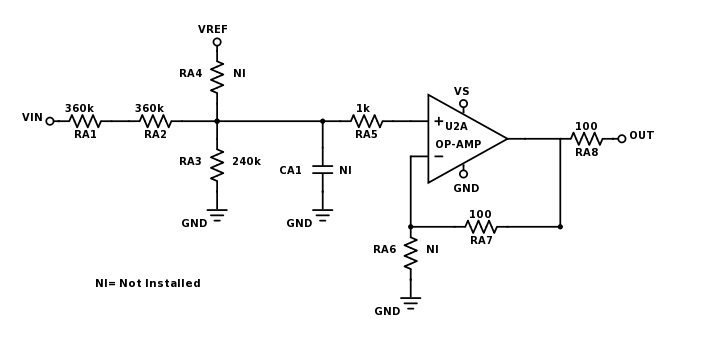
See Figure 3: Schematic for Each Channel
Divider-BIP10V: See Table 1 of the datasheet
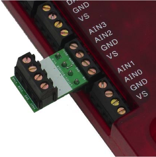
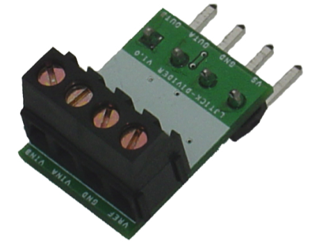
The 4-pin design plugs into the standard AIN/AIN/GND/VS screw terminal block found on all LabJacks except the original U12. Note that the best performance on the U3 or T7 is achieved with low-voltage inputs (labeled FIO and EIO).

VINA/VINB: These screw terminals are for the 2 single-ended channels of input analog voltages. Each voltage is multiplied by the fractional slope to provide a lower voltage to the LabJack. Note that the outputs of the LJTD are limited to about 0-3.5 volts.
GND: Same as LabJack ground. VINA/VINB must be referred to this ground.
VREF: A 2.5 volt reference voltage output. Internally this reference is used for level shifting, but very little current is used, leaving substantial current available to the user if a very accurate 2.5 volt reference is needed.

The above figure is a schematic for one channel of the LJTD, showing the standard factory installed values for UNI10V. The input/output relationship is described by the below equations, assuming the op-amp is in the default unity gain configuration.
General Equations for Figure 3:
Vout = Vin*Rpar/(R1+R2) + Rpar*Vref/R4
Slope = Rpar/(R1+R2)
Offset = Rpar*Vref/R4
Rpar = Rparallel = 1 / ( (1/(R1+R2) + 1/R3 + 1/R4) )
Simplified Equations for Unipolar Builds:
Vout = Vin*R3/(R1+R2+R3)
Slope = R3/(R1+R2+R3)
The resistors R1+R2, R3, and R4, can be changed to provide other ranges as shown in the table below.
The packages for resistors R1-R4 are 0805, while all other resistors and capacitors are 0603. The tolerance of the factory installed resistors is 0.05%, so a good option available from digikey.com is the Panasonic ERA-6ARW series.
The table shows the input voltage at an output voltage of 0.0 and 2.5 volts. It also shows the input voltage for an output voltage of 3.5 volts, as the internal buffer amplifier accepts a maximum input voltage of 3.5 volts when powered by VS=5.0 volts, and thus when the amp is configured for unity gain the maximum output voltage is 3.5 volts. The Slope and Offset columns go with the formula
VIN (OUT=0): This is the input voltage that results in an output voltage of 0.0 volts. The typical minimum output voltage of the LJTD is about 0.001 volts.
VIN (OUT=2.5): This is the input voltage that results in an output voltage of 2.5 volts.
VIN (OUT=3.5): This is the input voltage that results in an output voltage of 3.5 volts. The typical maximum output voltage of the LJTD is VS-1.5 which is about 3.5 volts.
Vout = Slope*Vin + Offset.
Ranges
Table 1. Ranges for divider circuit with different R1-R4
|
R1+R2 |
R3 |
R4 |
Slope |
Offset |
VIN (OUT=0) |
VIN (OUT=1.0) |
VIN (OUT=2.5) |
VIN (OUT=3.5) |
|
|
[ohms] |
[ohms] |
[ohms] |
[volts/volts] |
[volts] |
[volts] |
[volts] |
[volts] |
[volts] |
Name |
|
720k |
240k |
|
0.25 |
0 |
0 |
4.0 |
10.0 |
14.0 |
Div-4 |
|
720k |
180k |
|
0.2 |
0 |
0 |
5.0 |
12.5 |
17.5 |
Div-5 |
|
900k |
100k |
|
0.1 |
0 |
0 |
10.0 |
25.0 |
35.0 |
Div-10 |
|
876k |
36.5k |
|
0.04 |
0 |
0 |
25.0 |
62.5 |
87.5 |
Div-25 |
|
720k |
680k |
|
0.4857 |
0 |
0 |
2.1 |
5.1 |
7.2 |
UNI5V |
|
360k |
240k |
|
0.4 |
0 |
0 |
2.5 |
6.3 |
8.8 |
UNI6V |
|
720k |
240k |
|
0.25 |
0 |
0 |
4.0 |
10.0 |
14.0 |
UNI10V |
|
720k |
220k |
|
0.234 |
0 |
0 |
4.3 |
10.7 |
15.0 |
UNI11V |
|
720k |
100k |
|
0.122 |
0 |
0 |
8.2 |
20.5 |
28.7 |
UNI21V |
|
720k |
68k |
|
0.0863 |
0 |
0 |
11.6 |
29.0 |
40.6 |
UNI29V |
|
720k |
47k |
|
0.0613 |
0 |
0 |
16.3 |
40.8 |
57.1 |
UNI41V |
|
720k |
33k |
|
0.0438 |
0 |
0 |
22.8 |
57.0 |
79.9 |
UNI57V |
|
360k |
|
360k |
0.5 |
1.25 |
-2.5 |
-0.5 |
2.5 |
4.5 |
BIP2.5V |
|
360k |
240k |
180k |
0.2222 |
1.111 |
-5 |
-0.5 |
6.3 |
10.8 |
BIP5V |
|
720k |
240k |
180k |
0.125 |
1.25 |
-10 |
-2.0 |
10.0 |
18.0 |
BIP10V |
|
720k |
68k |
68k |
0.0451 |
1.194 |
-26.5 |
-4.3 |
29.0 |
51.1 |
BIP25V |
The labels in the Name column are used when ordering custom configurations.
U3: The LJTD is generally used with low-voltage channels on the U3-LV or U3-HV. The nominal input range of a low-voltage channel is 0-2.44 volts, so the input range provided by the LJTD is from the "VIN (OUT=0)" column to a little less than the "VIN (OUT=2.5)" column. For example, the UNI10V in this case will provide an input range of about 0 to 9.76 volts. If you set the U3 analog input to the "special" range it takes an input of about 0-3.6 volts, so the input range provided by the LJTD is from the "VIN (OUT=0)" column to the "VIN (OUT=3.5)" column. For example, the UNI10V in this case will provide an input range of about 0 to 14 volts.
U6/T7: The LJTD is used with the +/-10 or +/-1 volt range on the LabJack U6/T7. With the +/-10 volt range the full 0-3.5 volt output of the LJTD can be measured, but only 3.5/20 = 17.5% of the LabJack input range is used. With the +/-1 volt range, the 0 and 1 volt output columns above apply, and 50% of the LabJack input range is used.
UE9: The LJTD is used withe the 0-2.5 or 0-5 volt range on the UE9. The 0 and 2.5 volt output columns above use 100% of the 0-2.5 volt UE9 input range, or the 0 and 3.5 volt columns use 70% of the 0-5 volt UE9 input range.
Attenuating Higher Voltages
Due to the small trace spacing on the PCB, voltages beyond the options shown in the table above are not recommended. Instead, higher voltages can be handled by adding 1 or more external resistors in series with VIN. The extra voltage will be dropped across the external resistance such that the voltage applied to VIN is within specifications:
Simplified Equations for Unipolar Builds with External Resistor:
Vout = Vin*R3/(R1+R2+R3+Rext)
Slope = R3/(R1+R2+R3+Rext)
For example, say a 10 MΩ resistor such as the USF340-10.0M-0.01%-5PPM is used for Rext with the LJTick-Divider-25. That means the slope will be 36.5k / (876k + 36.5k + 10000k) = 0.003345, and thus a voltage of 747 volts will be divided down to 2.5 volts.
When working with a high voltage system and a USB device, consider adding a USB isolator. A mistake might damage the LabJack, but hopefully the isolator will protect the host computer.
Caution: The information in this section (Attenuating Higher Voltages) is presented for convenience, is not a feature of normal LabJack operation, and you are at your own risk when working with high voltages. High voltages are dangerous and only qualified individuals should work with high voltages. A mistake could easily result in damage to the LabJack, computer, and people.
Use with Digital Signals
The LJTD can be plugged in to a digital I/O block and used to condition digital signals. There are a couple reasons you might do this:
-
Higher Voltages: The LJTD-5 is perfect for handling 24 V signals. 24 divided by 5 is 4.8 volts, but the max output of the LJTD is about 3.5 volts, so the LabJack will see a 3.5 volt signal when the digital signal is driving 24 volts. The LJTD-4 works for 12V or 24V logic. A 12V signal will divide down to about 3.0V which is a logic high for any LabJack. A 24V signal will result in about 3.5V, as that is the max output of the LJTD, and that also is a good logic high for any LabJack.
-
Pull-Down Behavior: From the schematic in Figure 3 above, you can see that RA3 acts as a pull-down resistor. If the input (VIN) is disconnected or otherwise floating, the output of a unipolar LJTD will be near 0 volts.
Specifications
|
Parameter |
Conditions |
Min |
Typical |
Max |
Units |
|---|---|---|---|---|---|
|
General |
|
|
|
|
|
|
Vs, Supply Voltage (1) |
|
2.8 |
5 |
5.5 |
Volts |
|
Supply Current |
|
|
1.2 |
|
mA |
|
Operating Temperature |
|
-40 |
|
85 |
°C |
|
VREF |
|
|
|
|
|
|
Output Voltage |
|
2.495 |
2.5 |
2.505 |
Volts |
|
Initial Accuracy |
|
|
|
±0.2 |
% |
|
Maximum Output Current |
|
|
|
24 |
mA |
|
|
|
|
|
|
|
|
Op-Amp Buffer |
|
|
|
|
|
|
Typical Input Voltage Range |
|
-0.1 |
|
VS - 1.5 |
Volts |
|
Typical Output Voltage Range |
Load ≥ 100kΩ |
0.001 |
|
VS - 0.001 |
Volts |
|
|
|
|
|
|
|
|
Input/Output |
|
|
|
|
|
|
Slope Error |
|
|
|
±0.2 |
% |
|
Offset Error |
|
|
|
±0.2 |
% |
|
Input Impedance (2) |
UNI10V |
|
960 |
|
kΩ |
|
Input Bias current (2) |
VIN = 10V |
|
10 |
|
μA |
(1) The maximum input voltage to the buffer amplifier is VS-1.5, so for proper operation with signals up to 2.5 volts, VS must be greater than 4.0 volts.
(2) The input impedance and bias current is dominated by the input resistors not the buffer amplifier. The input bias current of the internal buffer amplifier is less than ±200 pA across the voltage range, which is an important number as far as sizing the input resistors to not create excessive offset.
CAD
Declaration of Conformity
Manufacturers Name: LabJack Corporation
Manufacturers Address: 6900 West Jefferson Ave Suite 110, Lakewood, CO 80235 USA
Declares that the product
Product Name: LJTick-Divider
Model Number: LJTD
conforms to the following Product Specifications:
EMC Directive: 89/336/EEC
EN 55011 Class A
EN 61326-1: General Requirements

