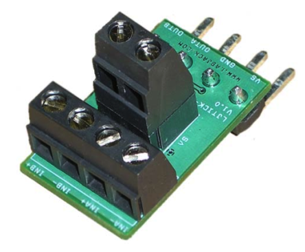
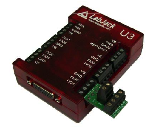
The LJTick-CurrentShunt (LJTCS) is a signal-conditioning module designed to convert 2x 4-20 mA current loop signals into voltage signals that vary from 0.472-2.360 volts. The 4-pin design plugs into the standard AnalogInput/AnalogInput/GND/VS screw terminal block found on many devices with non-isolated analog inputs, such as the U3, U6, UE9, T4, and T7. The major advantages of the LJTCS, compared to using a simple load resistor, are ease of use, high common-mode range, and lower voltage drop on the 4-20 mA signal.
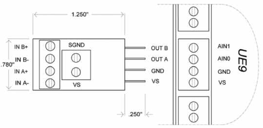
The pins shown on the right side of the LJTCS (Figure 1) connect to the LabJack. The VS/GND pins power the LJTCS, while the OUTA/OUTB pins send the output voltage signal to analog inputs on the LabJack.
Note that 4-20 mA corresponds to 0.472 to 2.36 volts, and thus on the U3-HV and T4 the low-voltage analog inputs (FIO/EIO) will provide the better results than the high-voltage analog inputs (AIN0-AIN3).
Following are descriptions of the LJTCS screw-terminal connections:
SGND: This terminal connects to LabJack ground (GND), with a 750 mA self-resetting thermal fuse in series. Often, the 4-20 mA sensor has its own power supply, and that supply ground needs to be connected to LabJack ground to provide a common reference. SGND allows that to be done, but protects from the risk of the external power supply dumping excess ground current through the LabJack.
VS: This is the same 5 volt output as the VS terminals on the LabJack itself. This is an output terminal, not an input. It can be used to provide 5 volt (nominal) power as needed.
INA+/INA- (or INB+/INB-): The 4-20 mA current loop should be connected to INA+ and INA- such that the current flows into INA+ and out of INA-. Each channel has a 5.9 Ω measurement resistor (0805, 0.10%, 50ppm), and the voltage across that resistor is amplified by x20. So 4 mA gives about 0.472 volts and 20 mA gives about 2.36 volts.
Relationship between output voltage and input current
I = V / (20 * 5.9) = V / 118
mA = 8.475 * volts
In addition to the 5.9 Ω shunt resistor, there is a self-resetting thermal fuse in series. The fuse is the MICROSMD005F-2 with a hold current of 50 mA and trip current of 150 mA. It has a typical resistance of 18 Ω (min=3.6 and max=50). It does not affect the measurement, but does affect how much voltage is dropped as the 4-20 mA signal passes through the LJTCS.
The common-mode input range of the LJTCS is -8 to +28 volts. That means that the voltage of each of the inputs must be within that range compared to LJTCS ground.
If the 4-20 mA signal does not have a common reference at all with the LJTCS, one needs to be made. One common way of doing this is by connecting ground from the sensor to SGND on the LJTCS. SGND has a fuse in series and then connects to normal GND. The fuse is a 750 mA self-resetting thermal fuse, and prevents other systems from using the LJTCS ground as their power ground.
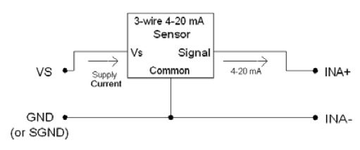
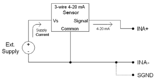
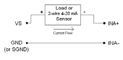
The following figures show typical connections. Figures 3 & 4 show typical connections with a 3-wire sourcing type sensor. This type of sensor sources the 4-20 mA signal, which is then returned to sensor ground. The common-mode voltage of INA- is 0, while the common-mode voltage of INA+ is equal to the signal loading of the LJTCS (typically 0.48 volts @ 20 mA).
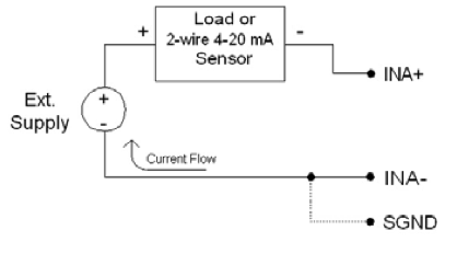
Figures 5 & 6 show typical connections with a 2-wire (loop-powered) sourcing type sensor. This type of sensor sources the 4-20 mA signal, which is then returned to sensor ground. The common-mode voltage of INA- is 0, while the common-mode voltage of INA+ is equal to the signal loading of the LJTCS.
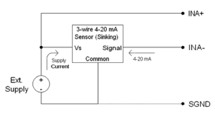
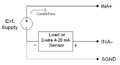
Figures 7 & 8 show typical connections with sinking type sensors. This type of sensor sinks the 4-20 mA signal, and thus the common-mode voltage of INA+ is equal to the full supply voltage and the common-mode voltage of INA- is equal to the supply voltage minus the signal loading of the LJTCS.
Troubleshooting
-
Do basic tests of the applicable AIN channel without the LJTCS connected. Connect a jumper wire from AINx to VS or GND, and make sure it reads ~5V or 0V as expected. See the Test an AIN Channel app note for more.
-
Note the discussion above about having a common reference. When you are using external supplies (Figures 4, 6, 7 and 8), those supplies must be referred to LabJack GND. If the supplies are not already referred (the DC output of an AC-DC supply is usually floating), make one connection from the common/negative of each power supply to SGND or GND on the LJTCS or LabJack.
-
Use a DMM to measure the voltage of IN+ and IN- versus GND. Both must be in the range of -8 to +28 volts versus GND.
-
Use a DMM to measure the voltage difference of IN+ versus IN-. The total input impedance of the LJTCS varies from 9 to 56 ohms, but the typical value is 24 ohms, and if you are putting 10 mA (for example) through 24 ohms you should measure a voltage difference of about 0.24 volts.
-
Use a DMM to measure the voltage of OUT/AIN versus GND. The output voltage should be 20*5.9*I, so if the current is 10 mA (for example) the output voltage should be about 1.18 volts.
-
Put a DMM in series with the IN+ terminal to see what it reports for current.
-
Remove the LJTCS from the LabJack and remove all I/O connections, then use a DMM to measure the resistance from IN+ to IN-. The total input impedance of the LJTCS varies from 9 to 56 ohms, but the typical value at room temperature is 24 ohms.
-
Rather than connecting your signal, do a basic test with a 1k resistor connecting VS to IN+ and a jumper from IN- to GND. This should result in roughly 5 mA (VS/1000), and then you can do the above measurements with that known current.
-
Too much noise? First step is to isolate the source of the noise to the LabJack, LJTick-CurrentShunt, or the signal itself. Do the above test with a resistor, but rather than VS (which might be noisy) use a battery (great) or DAC output (good to great depending on device) with an appropriate resistor to get a current around 5 mA.
Custom Ranges
The current on each channel flows into IN+, then through a self-resetting thermal fuse (F2/F3, MICROSMD005F-2), then through the 5.9 ohm 0805 0.1% sense resistor (R2/R5), and then back out IN-. The voltage across the sensor resistor is multiplied by 20 to provide the output signal. Some considerations if modifying R2/R5 to provide a custom range:
-
If you plan to measure over 50 mA, you will need to change or short out the fuse. Note that without the fuse if a low impedance voltage source is connected directly across IN+ and IN- there is high risk of damage.
-
The gain is provided by an AD8202. R3/R6 is the location for an 0805 feedback resistor (used to increase gain) and is normally not installed which means the gain is x20.
-
The AD8202 gain can be reduced using a resistor from A1/A2 to GND. The LJTCS has a 1000 pF capacitor C2/C4 from A1/A2 to GND, so that can be replaced with an 0603 resistor to reduce gain.
-
The typical output voltage of the AD8202 is about 0.02 to VS-0.2, so 0.02-4.80 volts if VS = 5.0.
-
The max recommended current due to the size of the PCB traces is 1 amp. This is a conservative limit and 1 amp is definitely no problem.
-
The burden voltage your signal must drive is the sum of the voltage drop across the fuse (varies from 3.6 to 50 ohms), the sensor resistor, and the PCB traces (typically less than 0.02 ohms).
Measuring Current App Note
For more information about measuring current, see the Measuring Current App Note.
-
Measuring current with a shunt resistor, Hall effect sensor or current transformer.
-
Measuring 4-20 mA with isolated analog inputs (e.g. LabJack T8).
-
Measuring currents other than 4-20 mA.
Specifications
|
Parameter |
Conditions |
Min |
Typical |
Max |
Units |
|
General |
|
|
|
|
|
|
Supply Voltage |
|
3.6 |
5 |
12 |
Volts |
|
Supply Current |
|
|
0.5 |
|
mA |
|
Operating temperature |
|
-40 |
|
85 |
°C |
|
|
|
|
|
|
|
|
Signal Specs |
|
|
|
|
|
|
Gain (1) |
|
|
20 |
|
V/V |
|
Sense Resistor |
|
|
5.9 |
|
Ohm (Ω) |
|
Gain Accuracy |
|
|
0.5 |
|
% |
|
Offset Accuracy |
|
|
2 |
|
mV |
|
Total Input Impedance (2) |
|
9 |
24 |
56 |
Ohm (Ω) |
|
Signal Loading (2) |
@ 20 mA |
|
0.48 |
|
Volts |
|
Common-Mode Range (3) |
VS = 5 V |
|
-8 to +28 |
|
Volts |
|
Typical Output For 4-20mA |
|
0.472 |
|
2.36 |
Volts |
|
Typical Output Range |
|
0.02 |
|
VS - 0.2 |
Volts |
|
Typical Input Range |
Vout = 0.02 - 4.8 V |
0.17 |
|
40.7 |
mA |
|
-3dB Bandwidth |
|
|
1200 |
|
Hz |
(1) The 4-20 mA signal passes through a sense resistor, and the voltage across that resistor is amplified to produce the output voltage signal. Thus the response of the LJTick-Current is 118 mV/mA.
(2) The total input impedance is the sum of the sense resistor and the thermal fuse resistance, and is typically 21-27 ohms at room temperature. The voltage dropped across this total impedance by the 4-20 mA signal is the loading.
(3) The voltage from IN+/IN- to GND must stay within the common-mode limits.
Drawings and CAD
Declaration of Conformity
Manufacturers Name: LabJack Corporation
Manufacturers Address: 6900 West Jefferson Ave Suite 110, Lakewood, CO 80235 USA
Declares that the product
Product Name: LabJack Tick Current Shunt
Model Number: LJTCS
conforms to the following Product Specifications:
EMC Directive: 89/336/EEC
EN 55011 Class A
EN 61326-1: General Requirements

