Production Status: no longer available ( NLA ). The LJTIA2 has been replaced by a newer, and simpler, LJTick-InAmp 3 (LJTIA3).
The LJTick-InAmp 2 (aka LJTIA2) is a signal-conditioning module that provides two instrumentation amplifiers ideal for low-level signals such as bridge circuits (strain gauges) and thermocouples. The LJTIA 2 has 5 gain settings per channel and two selectable output voltage offsets (Voffset). The 4-pin design plugs into the standard AIN/AIN/GND/VS screw-terminal block found on the LabJacks such as the U3, U6, UE9, T4, & T7.
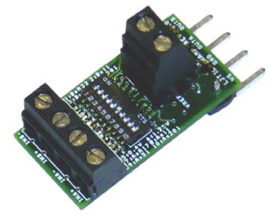
The pictures below show the LJTIA 2 by itself on the left and plugged into the U3 on the right.


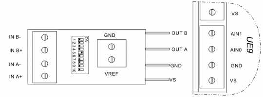
The block of 4 screw-terminals at the left edge of the LJTIA 2 (Figure 1 above) provides a positive and negative input for each differential channel. Towards the LabJack side of the LJTIA 2 is a pair of screw-terminals that provide a ground connection (GND) and a +2.50 volt reference (VREF). The reference is capable of sourcing enough current (see the Specifications section below) to function as the excitation voltage for most common bridge circuits.
Subsections
The following subsections have additional information relative to the LJTick-InAmp 2.
Dip Switches
In between the blocks of screw-terminals is a 10-position DIP switch used to specify gain and offset.
Table 1. DIP Switch Descriptions
|
Switch # |
Name |
Description |
|
|
1 |
BxR32 |
Custom gain determined by R32 |
Applies to channel B only. All off equals a gain of 1. |
|
2 |
Bx11 |
Gain of 11 |
|
|
3 |
Bx52 |
Gain of 51 |
|
|
4 |
Bx201 |
Gain of 201 |
|
|
5 |
0.4V |
Output offset of +0.4 volts. |
Voffset applies to both channels. Switch # 5 or 6 should always be on, but not both. |
|
6 |
1.25V |
Output offset of +1.25 volts. |
|
|
7 |
AxR17 |
Custom gain determined by R17 |
Applies to channel A only. All off equals a gain of 1. |
|
8 |
Ax11 |
Gain of 11 |
|
|
9 |
Ax51 |
Gain of 51 |
|
|
10 |
Ax201 |
Gain of 201 |
|
Each channel has a switch (numbers 1 & 7) that has been left without factory-installed gain resistors: R17 for channel A and R32 for channel B. Resistors can be installed by the end-user to provide custom gains according to G=1+(100k/R). For example, a resistance of 100 ohms would provide the maximum allowable gain of 1001. Also, multiple switches can be closed at the same time to get a few other gains (x61, x211, x251, and x261), as the gain settings resistors (10k, 2k, and 500) wind up in parallel. The packages for resistors R17 & R32 are 0805, while all other resistors and capacitors are 0603. The tolerance of the factory installed resistors is 0.1% & 25 ppm/degC, so consider the RG20P series from digikey.com (100ohm = RG20P100BCT).
Extending from the back of the LJTick-InAmp 2 are four pins. The first two pins provide +5 volt power and ground from the LabJack. The other two pins are the instrumentation amplifier outputs and connect to analog inputs on the LabJack. The four pins plug directly into the 5.0 mm spaced screw-terminals on the LabJack U3, UE9, or other future devices as shown in Figure 4.

Each channel on the LJTIA 2 has an AD623 instrumentation amplifier (in-amp) from Analog Devices. The allowable signal range (Vin) is determined by a combination of Gain, Voffset, Vcm, and Vout. See the Signal Range Tables in Appendix A.
Voffset: This is an offset voltage added to the in-amp output. If DIP switch #5 is on, the offset is +0.4 volts, and if DIP switch #6 is on, the offset is +1.25 volts. The same offset applies to both channels of the LJTick-InAmp 2. One offset must always be selected (0 volts is not an option), but both offsets should never be enabled at the same time. The +0.4 volt offset is generally used with signals that are mostly unipolar, while the +1.25 volt offset is generally used with bipolar signals.
Vcm: This is the common mode voltage of the differential inputs. For an in-amp, that is defined as the average of the common mode voltage of each input. For instance, if the negative input is grounded, and single-ended signal is connected to the positive input, Vcm is equal to Vin/2. Another common situation is when using a wheatstone bridge where VREF=2.5 is providing the excitation. In this case, each input is at about 1.25 volts compared to ground, and thus Vcm is about 1.25 volts.
Vin: This is the voltage difference between IN+ and IN-. In the following Signal Range Tables, the “Low” column is the minimum Vin where Vout is 10 mV or higher, the “High 2.5V” column is the maximum Vin where Vout is 2.5 volts or less, and the “High 4.5V” column is the maximum Vin where Vout is 4.5 volts or less.
Vout: Vout = (Vin * Gain) + Voffset. This is the single-ended (referred to ground) voltage output from the in-amp. Because of the power supply to the in-amp, the full output swing is about 0.01 volts to 4.5 volts. The “Low” and “High” columns in the Signal Range Tables give the output at the respective Vin.
Specifications
|
Parameter |
Conditions |
Min |
Typical |
Max |
Units |
|
General |
|
|
|
|
|
|
Supply Voltage |
|
3.6 |
5 |
5.5 |
volts |
|
Supply Current |
No Loads |
|
1.5 |
|
mA |
|
Operating Temperature |
|
-40 |
|
85 |
°C |
|
Signal Specs |
|
|
|
|
|
|
Gain Accuracy (1) |
|
|
0.35 |
1.2 |
% |
|
Offset Accuracy (1) |
G = 1 |
|
0.5 |
1.2 |
% |
|
|
G = 11 |
|
0.5 |
1.2 |
% |
|
|
G = 51 |
|
2.5 |
4.0 |
% |
|
|
G = 201 |
|
10 |
15.0 |
% |
|
Input Signal Limits (2) |
|
-0.15 |
|
VS - 1.5 |
volts |
|
Output Signal Limits (2) |
Load ≥ 10 kΩ |
0.01 |
|
VS - 0.5 |
volts |
|
Input Bias Current (3) |
|
|
17 |
|
nA |
|
Input Impedance |
|
|
2 |
|
GΩ |
|
Each Input vs. GND (4) |
Normal Operation |
|
|
-0.3 to +5.3 |
volts |
|
Each Input vs. GND (4) |
No Damage |
|
|
-10 to +15 |
volts |
|
-3 dB Bandwidth |
x1 |
|
18 |
|
kHz |
|
|
x11 |
|
18 |
|
kHz |
|
|
x51 |
|
18 |
|
kHz |
|
|
x201 |
|
10 |
|
kHz |
|
Vref |
|
|
|
|
|
|
Output Voltage |
|
2.495 |
2.50 |
2.505 |
volts |
|
Initial Accuracy |
|
|
0.2 |
|
% |
|
Current Output (5) |
For rated V accuracy |
0 |
|
25 |
mA |
(1) The max accuracy specs are the tested device limits and are expected to be met whether device is warmed up or not. Typical specs are what is normally seen with a warmed up device at room temperature. Gain and offset are very stable at a stable temperature, so a user-calibration can achieve accuracy much better than the specs listed here.
(2) The input signal limits are the simple limit of the voltage on each input terminal versus ground. The output signal limit is the simple typical limit of the voltage that can be produced on the output pins, and depends on load so see the AD623 datasheet for more information. The actual limits in most situations are more complex, as described in Appendix A of this datasheet.
(3) The current in/out of the input terminals is nanoamps from -0.3 to +5.3 volts. Beyond that range it increases up to 10mA at -10 or +15 volts.
(4) This is the limit of the voltage on any input terminal versus ground. See Appendix A for actual limits in different situations.
(5) Higher currents will not cause damage, but the reference voltage will start to sag. The reference output can handle a continuous short-circuit to ground and has a short-circuit current of about 45 mA typically.
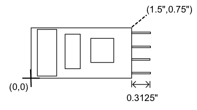
Dimensions

Declaration of Conformity
Manufacturers Name: LabJack Corporation
Manufacturers Address: 6900 West Jefferson Ave Suite 110, Lakewood, CO 80235 USA
Declares that the product
Product Name: LJTick-InAmp 2
Model Number: LJTIA 2
conforms to the following Product Specifications:
EMC Directive: 89/336/EEC
EN 55011 Class A
EN 61326-1: General Requirements
