Source Impedance: 50 Ω
Max Output Current: 20mA*
*See Appendix A-4 for details on voltage drop related to current draw.

|
Device |
Resolution (bits) |
Resolution (Volts) |
Source Impedance (Ω) |
Approx. Vout Min |
Approx. Vout Max |
|---|---|---|---|---|---|
|
T7 |
12 |
~1.2 mV |
50 |
0.0 |
5 |
|
T4 |
10 |
~5 mV |
50 |
0.0 |
5.0 |
|
T8 |
16 |
~160 µV |
50 |
-0.1 |
10.0 |
Overview
T-Series devices have two DACs (digital-to-analog converters, also known as analog outputs). Each DAC will set its output voltage according to the provided value. The output voltage is limited by the min and max range. The step size or granularity is limited by the resolution. For example: The T7's DACs have a range of 0-5V and resolution of 12-bits, the step size is then (5-0) / 212 ≈1.2 mV with a max of ~5 V and a minimum of ~0 V.
For electrical specifications, See Appendix A-4.
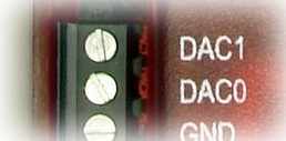
The T7 DACs appear both on the screw terminals and on the DB37 connector. These connections are electrically the same, and the user must exercise caution only to use one connection or the other, and not create a short circuit.
Device Control Basics
-
All T-series device features are controlled by reading and writing Modbus TCP registers via Modbus TCP (either directly or through our LJM library).
-
We have register descriptions throughout documentation detailing relevant register names, starting addresses, types, and access permissions (read/write).
-
See Section 3.0 Communication for other detailed communication information.
Register Listing
To set DAC output voltage, write to the following registers:
Output Range
T4/T7:
The DAC output amplifiers are designed so that the nominal maximum output is 5.0 volts. The actual maximum voltage can vary and will always be limited according to the supply voltage. To determine the actual max of each DAC, write an impossibly high value such as 6.0 to the DAC, and then read back the value. This is the expected full-scale output with no load and with a supply voltage greater than the returned value. If Vs is below the returned value, the maximum output will be reduced accordingly. The step size of the DACs will not be affected, instead the output voltage will stop increasing after the expected output reaches VS.
The output range is also limited by the ability of the output amps to drive near the power rails (0 and VS). They can drive quite close, especially at light load, but will never be able to drive all the way to exactly 0.0 or VS.
The output range is further limited under load by the drive ability of the output amp and the 50 ohms of source resistance. The latter is dominant at lower currents, so for example if you set a DAC to 4.000 volts and draw 2 mA from it, the output will be closer to 3.900 volts.
See Appendix A-4 for more information.
T8:
The DACs on the T8 use additional power systems to output voltage levels above and below the supply. This allows the T8 to output approximately -0.1 to 10 V as long as the supply voltage is within the valid operating range.
The DACs on the T8 have good load regulation. Very little voltage drop is expected up to 20mA, usually 1-2 mV.
See Appendix A-4 for more information.
To output voltages from -10 V to 10 V, the LJTick-DAC is a great solution.
Power-up Defaults
The power-up condition of the DACs can be configured by the user. From the factory, the DACs default to be enabled at minimum voltage (~0 V). Note that even if the power-up default for a line is changed to a different voltage or disabled, there is a delay of about 100 ms at power-up where the DACs are in the factory default condition.
Reading
A read of DACx returns the last value that was written to the DAC chip.
Protection
The analog outputs can withstand a continuous short-circuit to ground, even when set at maximum output.
Voltage should never be applied to the analog outputs, as they are voltage sources themselves. In the event that a voltage is accidentally applied to either analog output, they do have protection against transient events such as ESD (electrostatic discharge) and continuous overvoltage (or undervoltage) of a few volts.
10 Hz Square Wave Output
DAC1 can be configured to output a 10 Hz, 3.3 V square wave. Writing a 1 to DAC1_FREQUENCY_OUT_ENABLE will enable the 10 Hz output:
The square wave output will be disabled:
-
when 0 is written to DAC1_FREQUENCY_OUT_ENABLE,
-
when any value is written DAC1,
-
or when a stream-out channel targeting DAC1 is enabled.
T7 requires firmware version 1.0234 or later.
Increasing Output to ±10V
There is an accessory available from LabJack called the LJTick-DAC that provides a pair of 14-bit analog outputs with a range of ±10 volts. The LJTick-DAC plugs into any digital I/O block and thus many can be added to a T-series device.
Testing
A good way to test the DACs is to see if they output the expected voltage when loaded. The source impedance of the DACs is about 50 ohms, and that source impedance interacts with load impedance to form a voltage divider. Remove all user connections and connect a 470 ohm resistor from DAC# to GND. A voltage divider is formed such that:
Vout = Vset * 470 / (470 + 50) = Vset * 0.9
So whatever the DAC is set to, the output at the terminal should be about 10% less. You will see the 10% drop with test voltages up to about 4 volts. Above 4 volts, other effects come into play since this test is drawing substantial current from the DAC line.
