There is an accessory available from LabJack called the LJTick-DAC that provides a pair of 14-bit analog outputs with a range of ±10 volts. The LJTick-DAC plugs into any digital I/O block, and thus up to 10 of these can be used per UE9 to add 20 analog outputs.
The typical output range of the DACs is about 0.02 to 4.86 volts. For other unipolar ranges, an op-amp in the non-inverting configuration (Figure 2-3) can be used to provide the desired gain. For example, to increase the maximum output from 4.86 volts to 10.0 volts, a gain of 2.06 is required. If R2 (in Figure 2-3) is chosen as 100 kΩ, then an R1 of 93.1 kΩ is the closest 1% resistor that provides a gain greater than 2.06. The +V supply for the op-amp would have to be greater than 10 volts.
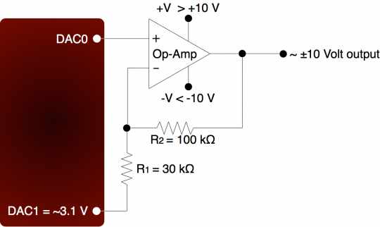
For bipolar output ranges, such as ±10 volts, a similar op-amp circuit can be used to provide gain and offset, but of course the op-amp must be powered with supplies greater than the desired output range (depending on the ability of the op-amp to drive it’s outputs close to the power rails). If these supplies are used to power the LT1490A op-amp (linear.com), which has rail-to-rail capabilities, the outputs could be driven very close to ±9.5 volts. If ±12 or ±15 volt supplies are available, then the op-amp might not need rail-to-rail capabilities to achieve the desired output range.
A reference voltage is also required to provide the offset. In the following circuit, DAC1 is used to provide a reference voltage. The actual value of DAC1 can be adjusted such that the circuit output is 0 volts at the DAC0 mid-scale voltage, and the value of R1 can be adjusted to get the desired gain. A fixed reference (such as 2.5 volts) could also be used instead of DAC1.
A two-point calibration should be done to determine the exact input/output relationship of this circuit. Refer to application note SLOA097 from ti.com for further information about gain and offset design with op-amps.

