
Features
The LJTick-InAmp3 (aka LJTIA3) is a signal-conditioning module with two independent channels. Each channel uses an instrumentation amplifier to amplify, and offset the signal while rejecting noise. This is ideal for small-voltage signals such as bridge circuits (strain gauges) and thermocouples.
The LJTIA 3 is available with gains of 11x, 51x or 201x and has a fixed output voltage offset of 1.25V. Custom gains and offsets are possible by replacing resistors on the Tick.
The 4-pin design plugs into the standard VS/GND/AIN/AIN screw-terminal block found on LabJacks such as the T4 and T7.
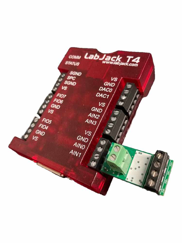
The pictures below show the LJTIA 3 by itself on the left and a possible connection with a T4 on the right.
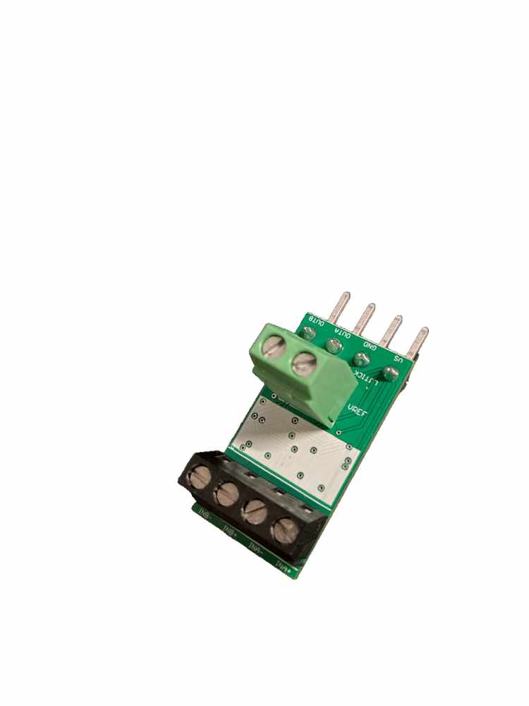
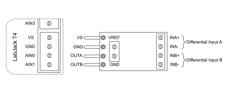
The block of 4 screw-terminals at the left edge of the LJTIA 3 (Figure 1 above) provides a positive and negative input for each differential channel. Towards the LabJack side of the LJTIA 3 is a pair of screw-terminals that provide a ground connection (GND) and a +2.50 volt reference (VREF). The reference is capable of sourcing enough current (see Specifications) to function as the excitation voltage for most common bridge circuits.
Gain Options
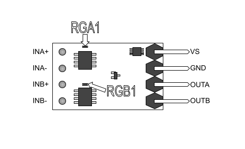
The gain for each instrument amplifier is set by a gain resistor. The gain from InA+/InA- to OUTA is determined by RGA1 and the gain from InB+/InB- to OUTB is determined by RGB1. These resistors can be found towards the input side of the LJTIA 3 directly above their corresponding instrumentation amplifiers (See Figure 3). The gain resistor values can be calculated according to:
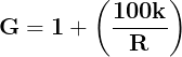
(For more info see the amplifier datasheet)
LabJack provides LJTIA 3s with one of three possible pre-configured gain options:
-
11x, where RGA1 = RGB1 = 10k
-
51x, where RGA1 = RGB1 = 2k
-
201x, where RGA1 = RGB1 = 500.
Additional gains (1 ≤ G ≤ 1000) can be achieved by replacing RGA1 and RGB1 with 0.1% tolerance 0603 package resistors with values according to Equation 1. NOTE: Unity 1x gain can be achieved by removing RGA1 or RGB1 completely.
The three default gain options of 11x, 51x, and 201x lead to the following transfer functions to calculate VOUT on either channel:
VOUTA=[(VINA+-VINA-) X 11] + 1.25V
Equation 2a: Transfer Function With 11x Gain (RGA1 = RGB1 = 10kΩ) .
VOUTA=[(VINA+-VINA-) X 51] + 1.25V
Equation 2b: Transfer Function With 51x Gain (RGA1 = RGB1 = 2000Ω) .
VOUTA=[(VINA+-VINA-) X 201] + 1.25V
Equation 2c: Transfer Function With 201x Gain (RGA1 = RGB1 = 500Ω) .
Pinout
Extending from the back of the LJTick-InAmp 3 are four pins. The first two pins provide +5 volt power and ground from the LabJack. The other two pins are the instrumentation amplifier outputs and connect to analog inputs on the LabJack. The four pins plug directly into the 5.0 mm spaced screw-terminals on the LabJack U-Series, T4, T7 or other future devices as shown in Figure 4.
Signal Names
Each channel on the LJTIA 3 has an AD623 instrumentation amplifier (in-amp) from Analog Devices. The allowable signal range (Vin) is determined by a combination of Gain, Voffset, Vcm, and Vout. See the Signal Range Tables in Appendix A.
Voffset: This is a fixed offset voltage of 1.25V added to the in-amp output.
Vcm: This is the common mode voltage of the differential inputs. For an in-amp, that is defined as the average of the common mode voltage of each input. For instance, if the negative input is grounded, and a single-ended signal is connected to the positive input, Vcm is equal to Vin/2. Another common situation is when using a wheatstone bridge where VREF=2.5 is providing the excitation. In this case, each input is at about 1.25 volts compared to ground, and thus Vcm is about 1.25 volts.
Vin: This is the voltage difference between IN+ and IN-. In the following Signal Range Tables, the “Low” column is the minimum Vin where Vout is 10 mV or higher, the “High 2.5V” column is the maximum Vin where Vout is 2.5 volts or less, and the “High 4.5V” column is the maximum Vin where Vout is 4.5 volts or less.
Vout: Vout = (Vin * Gain) + Voffset. This is the single-ended (referred to ground) voltage output from the in-amp. Because of the power supply to the in-amp, the full output swing is about 0.01 volts to 4.5 volts. The “Low” and “High” columns in the Signal Range Tables give the output at the respective Vin.
Specifications
|
Parameter |
Conditions |
Min |
Typical |
Max |
Units |
|
General |
|
|
|
|
|
|
Supply Voltage |
|
3.6 |
5 |
5.5 |
volts |
|
Supply Current |
No Load |
|
1.5 |
|
mA |
|
|
Operational |
|
|
6 |
mA |
|
Operating Temperature |
|
-40 |
|
85 |
°C |
|
Signal Specs |
|
|
|
|
|
|
Gain Accuracy (1) |
|
|
0.35 |
1.2 |
% |
|
Offset Accuracy (1) |
G = 11 |
|
0.5 |
1.2 |
% |
|
|
G = 51 |
|
2 |
5 |
|
|
|
G = 201 |
|
10 |
15 |
% |
|
Input Signal Limits |
|
-0.15 |
|
Vs-1.5 |
volts |
|
Output Signal Limits |
Load >= 10k |
0.2 |
|
Vs-0.5 |
volts |
|
Input Bias Current |
|
|
17 |
|
nA |
|
Input Impedance |
|
|
2 |
|
GΩ |
|
Each Input vs. GND |
|
-0.3 |
|
5.3 |
|
|
Each Input vs. GND |
|
-10 |
|
15 |
|
|
-3dB Bandwidth |
G = 11 |
|
18 |
|
kHz |
|
|
G = 201 |
|
10 |
|
kHz |
|
Vref |
|
|
|
|
|
|
Output Voltage |
|
2.495 |
2.50 |
2.505 |
volts |
|
Initial Accuracy |
|
|
0.2 |
|
% |
|
Current Output |
|
|
20 |
|
mA |
(1) The max accuracy specs are the tested device limits and are expected to be met whether device is warmed up or not. Typical specs are what is normally seen with a warmed up device at room temperature. Gain and offset are very stable at a stable temperature, so a user-calibration can achieve accuracy much better than the specs listed here.
Dimensions and CAD
Differences From LJTIA 2
The main difference from the previous LJTIA 2 is that the gain and offset are no longer set with dip switches. The offset is always at 1.25 V and the gain can be modified by swapping out gain resistors as described above.
Operation Testing
The following procedures can be used to test an LJTick-InAmp Revision 3.
Some DMMs may not have adequate resolution to measure less than 1 mV, which may be a problem for the DMM measurements in the tests below.
GND Test
-
Remove all signals from the LJTick-InAmp, and jumper all 4 inputs (INA+/INA-/INB+/INB-) to GND.
-
Measure the voltage between INA+ and INA- with a DMM and make a note of the value. This reading (VinA) should be close to 0 V since both inputs are shorted to GND. Repeat this step to measure between INB+ and INB-.
-
Check that the LJTick-InAmp offset is correct. If the DMM measurements were close to 0V, the output of the LJtick-InAmp (OUTA and OUTB) should be close to the offset voltage value of 1.25 V. More precisely, the output should follow this formula:
Vout = Vin * gain + 1.25
Wheregainis the gain configuration of your LJTick-InAmp andVinis the voltage you measured between the inputs in step 2. You can start by reading the output voltage (between OUTA or OUTB and GND) with a DMM. Also check that the output voltage looks correct by taking AIN reading using LabJack configuration software (Kipling for T-series devices or LJControlPanel for UD devices). For example, if the LJTick-InAmp is connected to AIN4 and AIN5, the voltage on AIN4 corresponds to OUTA and the voltage on AIN5 corresponds to OUTB.
DAC0 Test
-
Remove all signals from the LJTick-InAmp and connect INA+ to DAC0.
-
Connect a 100 Ω resistor between INA+ and INA-. Connect a 100 kΩ resistor between INA- and GND. This creates a voltage divider between INA+ and INA- with the following relationship:
Vout = VDAC0 * 100 / (100+50+100000)
Note that the value of 50 in the denominator is a stand in for the DAC output impedance, and it could be different depending on your device. The value should not matter much for this test, but the DAC specifications in your device datasheet could be used to verify the actual DAC output impedance. -
Set DAC0 to 1 V using the appropriate LabJack configuration software. This should produce a voltage of approximately 0.99 mV between INA+ and INA-.
-
Use a DMM to verify the voltage between INA+ and INA-. Make note of the value, it is VinA. There will be some error in both the resistor values and the DAC0 voltage, so don’t fret if the measured voltage is a little bit off from the expected value.
-
Measure the voltage of OUTA. It should follow this formula:
VoutA = VinA * gain + 1.25
Wheregainis the gain configuration of your LJTick-InAmp andVinAis the voltage you measured between the inputs in step 4. You can start by reading the output voltage (between OUTA or OUTB and GND) with a DMM. Also check that the output voltage looks correct by taking AIN reading using LabJack configuration software (Kipling for T-series devices or LJControlPanel for UD devices). For example, if the LJTick-InAmp is connected to AIN4 and AIN5, the voltage on AIN4 corresponds to OUTA and the voltage on AIN5 corresponds to OUTB. -
Change the voltage on DAC0 to 2V. This should approximately double the voltage of VinA. Repeat step 4 and step 5 to verify that you see the expected results.
-
Repeat all steps to test INB+, INB-, OUTB.
Different DAC0 voltages and resistors may be used in the DAC0 test, but care must be taken to account for any changes in the formulas used, and to ensure that the input and output voltages are within the signal ranges of the LJTick-InAmp.